How Solar Panels Are Made: From Silicon to Rooftop
Discover how solar panels are manufactured, from raw silicon purification to finished modules. Understand the technology powering your roof.
From Sand to Electricity
Every solar panel begins its life as ordinary sand. The journey from raw silica to a finished solar module capable of generating clean electricity for 30 years is a fascinating process that combines metallurgy, chemistry, and precision engineering.
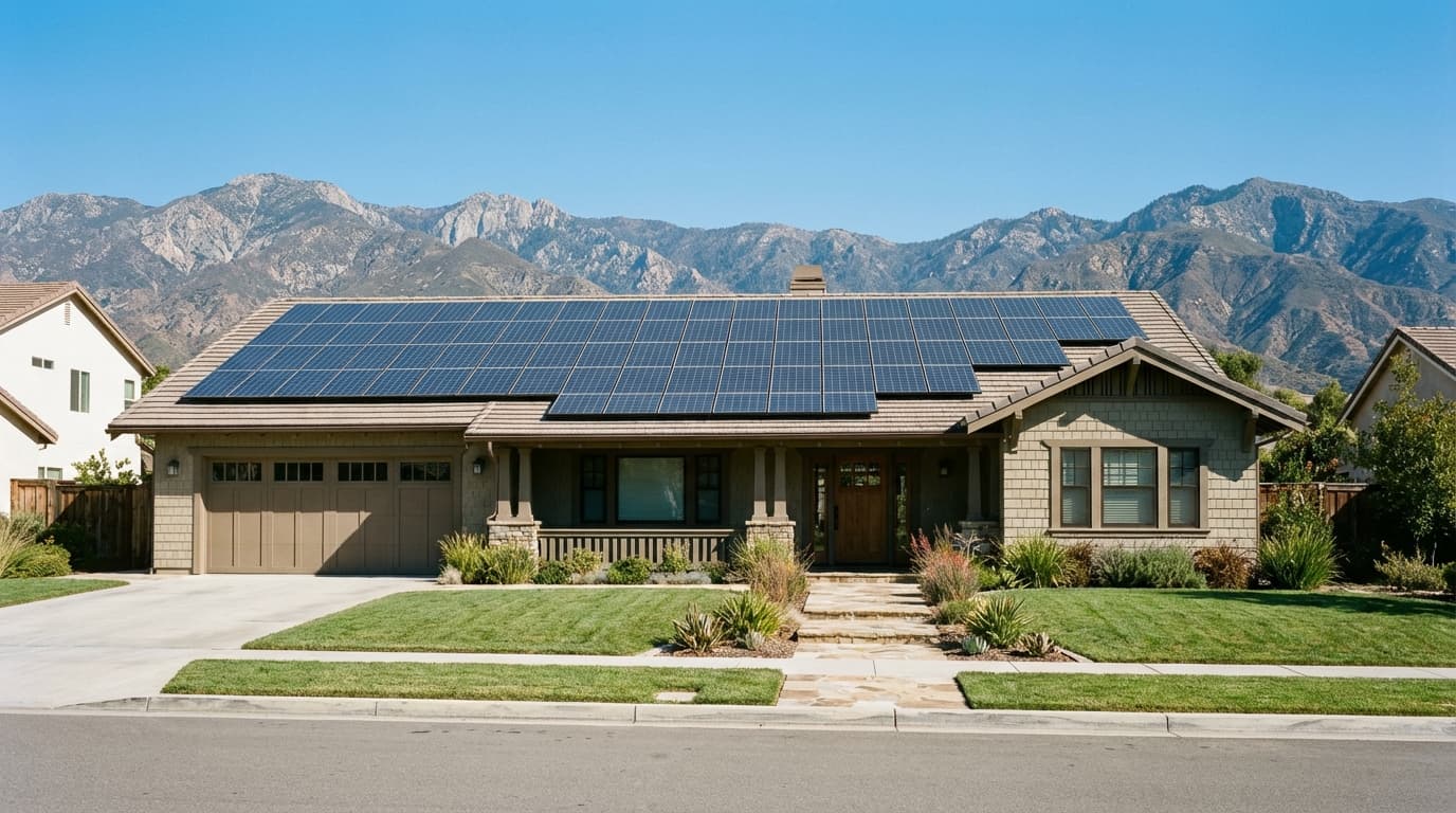
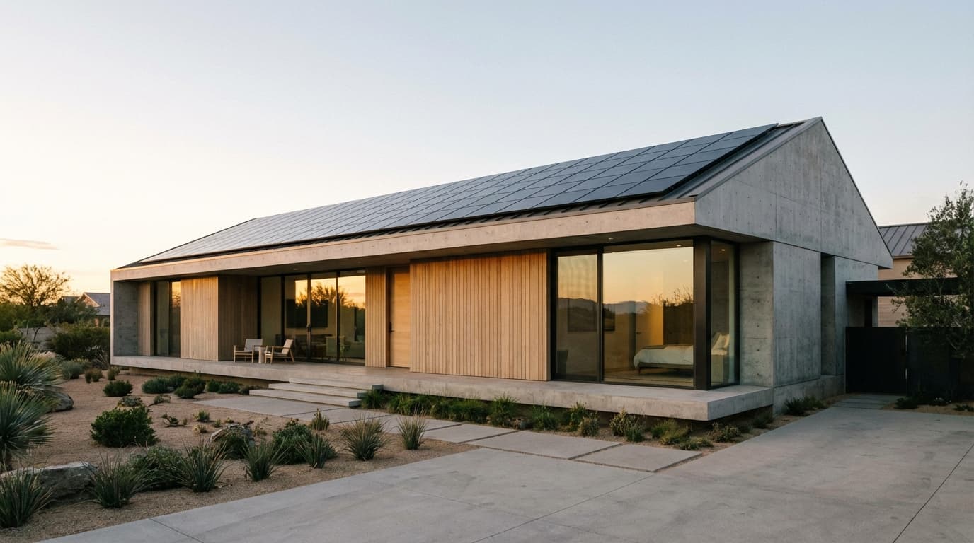
Understanding how solar panels are made gives you a deeper appreciation for the technology on your roof and helps you evaluate the quality differences between manufacturers.
Step 1: Silicon Purification
Mining Quartz
Solar-grade silicon starts as quartz (silicon dioxide, SiO2), one of the most abundant minerals on Earth. Quartz is mined from deposits around the world, with major sources in Brazil, Madagascar, and the United States.
Producing Metallurgical-Grade Silicon
The quartz is heated to approximately 2,000 degrees Celsius in an electric arc furnace with carbon (usually in the form of charcoal or coal). The carbon bonds with the oxygen, leaving behind metallurgical-grade silicon that is about 98 to 99 percent pure.
Refining to Solar-Grade Silicon
For solar cells, silicon must be 99.9999 percent pure (known as six nines purity). The Siemens process achieves this by converting metallurgical-grade silicon into trichlorosilane gas, purifying the gas through distillation, and then depositing high-purity silicon onto heated rods.
The result is polysilicon, a chunky, rock-like material with an intense metallic luster. This polysilicon is the foundation of nearly all solar cells manufactured today.
Step 2: Crystal Growing
Monocrystalline Ingots (Czochralski Process)
For monocrystalline solar cells, chunks of polysilicon are melted in a crucible at 1,425 degrees Celsius. A single crystal seed is dipped into the molten silicon and slowly pulled upward while rotating. As it rises, silicon atoms attach to the seed in a perfectly ordered crystal lattice, forming a large cylindrical ingot.
A typical ingot is 200 to 300 millimeters in diameter and up to 2 meters long, weighing 150 to 300 kilograms. The entire pulling process takes 2 to 3 days to complete.
Polycrystalline Blocks (Directional Solidification)
For polycrystalline cells, molten silicon is simply poured into a large square mold and allowed to cool slowly. As it solidifies, many small crystals form throughout the block. The resulting ingot has a characteristic grain boundary pattern visible as the blue speckled appearance of polycrystalline panels.

Step 3: Wafer Slicing
The silicon ingots are sliced into extremely thin wafers using diamond wire saws. Modern wafers are typically 150 to 180 micrometers thick, thinner than a human hair (about 70 micrometers) but still thick enough to absorb sunlight effectively.
Diamond wire sawing is a precision process that must balance wafer thinness (less silicon waste) against structural integrity (wafers must survive handling and processing). Despite improvements, the sawing process still wastes about 30 percent of the silicon as kerf loss, though researchers are working to reduce or eliminate this waste.
Step 4: Cell Fabrication
Texturing
The wafer surface is chemically etched to create a textured surface with tiny pyramidal structures. This texturing reduces light reflection from about 30 percent to less than 10 percent, ensuring more photons enter the cell.
Diffusion and Doping
To create the p-n junction that generates electricity, the wafer is processed with specific dopants. For traditional p-type cells, the wafer (already doped with boron) receives a phosphorus diffusion on the front surface, creating an n-type layer. The boundary between these layers is the p-n junction where the photovoltaic effect occurs.
Modern N-type cells (TOPCon, HJT) start with a phosphorus-doped wafer and add boron to the rear, offering improved efficiency and lower degradation.
Anti-Reflective Coating
A thin layer of silicon nitride is deposited on the cell surface using plasma-enhanced chemical vapor deposition (PECVD). This coating gives solar cells their characteristic blue or black color and reduces reflection to less than 2 percent.
Metallization
Silver paste is screen-printed in thin lines (busbars and fingers) on the cell's front surface and aluminum paste on the rear. The cell is then fired in a furnace at approximately 800 degrees Celsius, sintering the metal paste into conductive contacts that collect the generated electricity.
The silver fingers must be thin enough to minimize shading while wide enough to carry current efficiently. This balance is a key area of ongoing research and development.

Step 5: Module Assembly
Cell Sorting and Stringing
Finished cells are tested and sorted by electrical output. Cells with similar performance characteristics are grouped together (binned) to maximize module efficiency. Cells are then connected in series using thin copper ribbons soldered to the busbars.
A typical residential panel contains 60 or 72 half-cut cells (120 or 144 half-cells), connected in series strings that produce the module's rated voltage.
Lamination
The cell strings are sandwiched between layers in this order:
This sandwich is placed in a laminator and heated to 140 to 150 degrees Celsius under vacuum. The encapsulant melts and cross-links, permanently bonding all layers together.
Framing and Junction Box
An aluminum frame is attached around the laminate edges, providing structural rigidity and mounting points. A junction box is attached to the rear, housing bypass diodes and providing connection terminals for wiring.
Testing and Quality Control
Every finished panel is flash-tested under standard test conditions (1,000 W/m2 irradiance, 25 degrees Celsius cell temperature, AM 1.5 spectrum) to measure its actual power output. Panels are rated and labeled based on these measurements.
Additional quality tests include electroluminescence imaging (to detect invisible micro-cracks), insulation resistance testing, and visual inspection for cosmetic defects.
The Scale of Modern Manufacturing
Modern solar panel factories are massive operations. The largest facilities, operated by companies like LONGi, Jinko, and Trina, produce 30 to 50 gigawatts of panels per year, enough to power millions of homes. These factories run 24 hours a day, 7 days a week, with highly automated production lines that minimize human handling and maximize consistency.

Environmental Footprint
The energy payback time for a solar panel, the time it takes for the panel to generate as much energy as was used to manufacture it, is approximately 1 to 2 years in most U.S. locations. Given a 25 to 30 year lifespan, a solar panel generates 12 to 30 times more energy than was used to create it.
Manufacturing does involve some hazardous chemicals and significant energy consumption, but the lifecycle environmental impact is far lower than any fossil fuel electricity source.
The Bottom Line
The next time you look at a solar panel, you are seeing the result of an extraordinary manufacturing process that transforms one of Earth's most common elements into a clean energy generator that works silently for decades.
Understanding how panels are made helps you appreciate the quality differences between brands. Higher-quality manufacturing processes, purer silicon, better encapsulants, and more rigorous testing all contribute to panels that perform better and last longer.
Explore your solar options with SmartEnergyUSA and get connected with installers who offer panels from the world's best manufacturers. Get a free quote today.